- 您现在的位置:买卖IC网 > Sheet目录1917 > DSPIC30F4013-30I/ML (Microchip Technology)IC DSPIC MCU/DSP 48K 44QFN
2010 Microchip Technology Inc.
DS70138G-page 131
dsPIC30F3014/4013
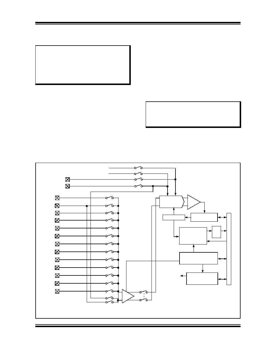
19.0
12-BIT ANALOG-TO-DIGITAL
CONVERTER (ADC) MODULE
The 12-bit Analog-to-Digital Converter (ADC) allows
conversion of an analog input signal to a 12-bit digital
number. This module is based on a Successive
Approximation Register (SAR) architecture and pro-
vides a maximum sampling rate of 200 ksps. The A/D
module has up to 16 analog inputs which are multi-
plexed into a sample and hold amplifier. The output of
the sample and hold is the input into the converter
which generates the result. The analog reference volt-
age is software selectable to either the device supply
voltage (AVDD/AVSS) or the voltage level on the
(VREF+/VREF-) pin. The A/D converter has a unique
feature of being able to operate while the device is in
Sleep mode with RC oscillator selection.
The A/D module has six 16-bit registers:
A/D Control Register 1 (ADCON1)
A/D Control Register 2 (ADCON2)
A/D Control Register 3 (ADCON3)
A/D Input Select Register (ADCHS)
A/D Port Configuration Register (ADPCFG)
A/D Input Scan Selection Register (ADCSSL)
The ADCON1, ADCON2 and ADCON3 registers
control the operation of the A/D module. The ADCHS
register selects the input channels to be converted. The
ADPCFG register configures the port pins as analog
inputs or as digital I/O. The ADCSSL register selects
inputs for scanning.
The block diagram of the 12-bit A/D module is shown in
FIGURE 19-1:
12-BIT A/D FUNCTIONAL BLOCK DIAGRAM
Note:
This data sheet summarizes features of
this group of dsPIC30F devices and is not
intended to be a complete reference
source. For more information on the CPU,
peripherals,
register
descriptions
and
general device functionality, refer to the
“dsPIC30F Family Reference Manual”
(DS70046).
Note:
The SSRC<2:0>, ASAM, SMPI<3:0>,
BUFM and ALTS bits, as well as the
ADCON3 and ADCSSL registers, must
not be written to while ADON = 1. This
would lead to indeterminate results.
Comparator
12-Bit SAR
Conversion Logic
VREF+
DAC
Da
ta
16-Word, 12-Bit
Dual Port
RAM
B
u
s
I
n
te
rf
ac
e
AN12
0000
0101
0111
1001
1100
0001
0010
0011
0100
0110
1000
1010
1011
AN8
AN9
AN10
AN11
AN4
AN5
AN6
AN7
AN0
AN1
AN2
AN3
CH0
AN1
VREF-
Sample/Sequence
Control
Sample
Input MUX
Control
Input
Switches
S/H
AVSS
AVDD
Fo
rm
a
t
Note:
The ADCHS, ADPCFG and ADCSSL registers allow the application to configure AN13-AN15 as analog input
pins. Since these pins are not physically present on the device, conversion results from these pins will read ‘0’.
发布紧急采购,3分钟左右您将得到回复。
相关PDF资料
DSPIC30F5013-30I/PT
IC DSPIC MCU/DSP 66K 80TQFP
DSPIC30F5015-30I/PT
IC DSPIC MCU/DSP 66K 64TQFP
DSPIC30F6010-20E/PF
IC DSPIC MCU/DSP 144K 80TQFP
DSPIC30F6010A-30I/PF
IC DSPIC MCU/DSP 144K 80TQFP
DSPIC30F6013A-30I/PF
IC DSPIC MCU/DSP 132K 80TQFP
DSPIC30F6014-30I/PF
IC DSPIC MCU/DSP 144K 80TQFP
DSPIC33EP512MU814-I/PL
IC DSC 16BIT 512KB 144LQFP
DSPIC33EP64MC504-E/TL
IC DSC 16BIT 64KB FLASH 44-VTLA
相关代理商/技术参数
DSPIC30F4013-30I/P
功能描述:数字信号处理器和控制器 - DSP, DSC General Purpose RoHS:否 制造商:Microchip Technology 核心:dsPIC 数据总线宽度:16 bit 程序存储器大小:16 KB 数据 RAM 大小:2 KB 最大时钟频率:40 MHz 可编程输入/输出端数量:35 定时器数量:3 设备每秒兆指令数:50 MIPs 工作电源电压:3.3 V 最大工作温度:+ 85 C 封装 / 箱体:TQFP-44 安装风格:SMD/SMT
DSPIC30F4013-30I/P
制造商:Microchip Technology Inc 功能描述:16BIT MCU-DSP 30MHZ 30F4013 DIP40
DSPIC30F4013-30I/PT
功能描述:数字信号处理器和控制器 - DSP, DSC General Purpose RoHS:否 制造商:Microchip Technology 核心:dsPIC 数据总线宽度:16 bit 程序存储器大小:16 KB 数据 RAM 大小:2 KB 最大时钟频率:40 MHz 可编程输入/输出端数量:35 定时器数量:3 设备每秒兆指令数:50 MIPs 工作电源电压:3.3 V 最大工作温度:+ 85 C 封装 / 箱体:TQFP-44 安装风格:SMD/SMT
DSPIC30F4013-30I/PT
制造商:Microchip Technology Inc 功能描述:DIGITAL SIGNAL CONTROLLER 16 BIT ((NW))
dsPIC30F4013T-20E/ML
功能描述:数字信号处理器和控制器 - DSP, DSC 44LD 20MIPS 48 KB RoHS:否 制造商:Microchip Technology 核心:dsPIC 数据总线宽度:16 bit 程序存储器大小:16 KB 数据 RAM 大小:2 KB 最大时钟频率:40 MHz 可编程输入/输出端数量:35 定时器数量:3 设备每秒兆指令数:50 MIPs 工作电源电压:3.3 V 最大工作温度:+ 85 C 封装 / 箱体:TQFP-44 安装风格:SMD/SMT
dsPIC30F4013T-20E/PT
功能描述:数字信号处理器和控制器 - DSP, DSC 20MIPS 48 KB RoHS:否 制造商:Microchip Technology 核心:dsPIC 数据总线宽度:16 bit 程序存储器大小:16 KB 数据 RAM 大小:2 KB 最大时钟频率:40 MHz 可编程输入/输出端数量:35 定时器数量:3 设备每秒兆指令数:50 MIPs 工作电源电压:3.3 V 最大工作温度:+ 85 C 封装 / 箱体:TQFP-44 安装风格:SMD/SMT
DSPIC30F4013T-20I/ML
功能描述:IC DSPIC MCU/DSP 48K 44QFN RoHS:否 类别:集成电路 (IC) >> 嵌入式 - 微控制器, 系列:dsPIC™ 30F 产品培训模块:XLP Deep Sleep Mode
8-bit PIC® Microcontroller Portfolio 标准包装:22 系列:PIC® XLP™ 18F 核心处理器:PIC 芯体尺寸:8-位 速度:48MHz 连通性:I²C,SPI,UART/USART,USB 外围设备:欠压检测/复位,POR,PWM,WDT 输入/输出数:14 程序存储器容量:8KB(4K x 16) 程序存储器类型:闪存 EEPROM 大小:256 x 8 RAM 容量:512 x 8 电压 - 电源 (Vcc/Vdd):1.8 V ~ 5.5 V 数据转换器:A/D 11x10b 振荡器型:内部 工作温度:-40°C ~ 85°C 封装/外壳:20-DIP(0.300",7.62mm) 包装:管件 产品目录页面:642 (CN2011-ZH PDF) 配用:DV164126-ND - KIT DEVELOPMENT USB W/PICKIT 2DM164127-ND - KIT DEVELOPMENT USB 18F14/13K50AC164112-ND - VOLTAGE LIMITER MPLAB ICD2 VPP
DSPIC30F4013T-20I/PT
功能描述:IC DSPIC MCU/DSP 48K 44TQFP RoHS:否 类别:集成电路 (IC) >> 嵌入式 - 微控制器, 系列:dsPIC™ 30F 产品培训模块:XLP Deep Sleep Mode
8-bit PIC® Microcontroller Portfolio 标准包装:22 系列:PIC® XLP™ 18F 核心处理器:PIC 芯体尺寸:8-位 速度:48MHz 连通性:I²C,SPI,UART/USART,USB 外围设备:欠压检测/复位,POR,PWM,WDT 输入/输出数:14 程序存储器容量:8KB(4K x 16) 程序存储器类型:闪存 EEPROM 大小:256 x 8 RAM 容量:512 x 8 电压 - 电源 (Vcc/Vdd):1.8 V ~ 5.5 V 数据转换器:A/D 11x10b 振荡器型:内部 工作温度:-40°C ~ 85°C 封装/外壳:20-DIP(0.300",7.62mm) 包装:管件 产品目录页面:642 (CN2011-ZH PDF) 配用:DV164126-ND - KIT DEVELOPMENT USB W/PICKIT 2DM164127-ND - KIT DEVELOPMENT USB 18F14/13K50AC164112-ND - VOLTAGE LIMITER MPLAB ICD2 VPP